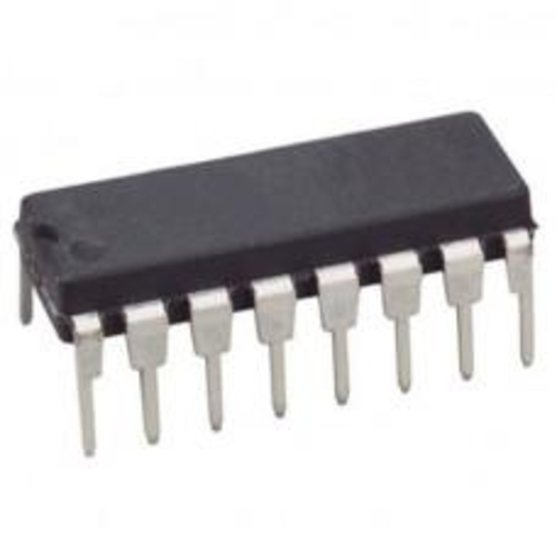
CD4099 – 8 bit Addressable Latch IC
The CD4099 8-bit addressable latch IC is a serial-input, parallel-output storage register that can perform a variety of functions.Data are inputted to a particular bit in the latch when that bit is addressed (by means of input A0, A1, A2) and when WRITE DISABLE is at a low level. When WRITE DISABLE is high, data entry is inhibited; however, all 8 outputs can be continuously read independently of WRITE DISABLE and address inputs.
A master RESET input is available, which resets all bits to a logic “0” level when RESET and WRITE DISABLE is at a high level. When RESET is at a high level, and WRITE RESET is at a low level, the latch acts as a 1-of-8 demultiplexer; the bit that is addressed has an active output that follows the data input, while all unaddressed bits are held to a logic “0” level.
The CD4099 types are supplied in 16-lead hermetic dual-in-line ceramic packages (F3A suffix), 16-lead dual-in-line plastic packages (E suffix), 16-lead small-outline packages (M, M96, MT, and NSR suffixes), and 16-lead thin shrink small-outline packages (PW and PWR suffixes).
check out :Quad NOR R-S Latch Tri-state IC – CD4043
Pinout:
| Pin No | Pin Name | Description |
|---|---|---|
| 1 | Q7 | Output Pin 7 of Latch |
| 2 | CL | Clear Output Pin |
| 3 | D | Data Input |
| 4 | E | Enable Pin |
| 5 | A0 | Input Pin 0 of Latch |
| 6 | A1 | Input Pin 1 of Latch |
| 7 | A2 | Input Pin 2 of Latch |
| 8 | VSS | Source Supply |
| 9 | Q0 | Output Pin 0 of Latch |
| 10 | Q1 | Output Pin 1 of Latch |
| 11 | Q2 | Output Pin 2 of Latch |
| 12 | Q3 | Output Pin 3 of Latch |
| 13 | Q4 | Output Pin 4 of Latch |
| 14 | Q5 | Output Pin 5 of Latch |
| 15 | Q6 | Output Pin 6 of Latch |
| 16 | VDD | Drain Supply |
Applications:
- Multi-line decoders
- A/D converters


Reviews
There are no reviews yet.